What Sets Laser Job Apart
40 Years of Dedication to
Laser Micromachining
Considering material, geometry, tolerances, production volume,
and other critical requirements,
we recommend the optimal machining solution for your application.
“Not sure it’s possible?”
Bring us the challenge first.
Laser Job’s Laser Technology
Can Help
Solve Your Most Complex Challenges!
01 Question What can you machine?
We deliver what others can’t
and respond to every inquiry quickly
ANSWER
Volume Production & Throughput
Achieve Both Quality and Cost Efficiency
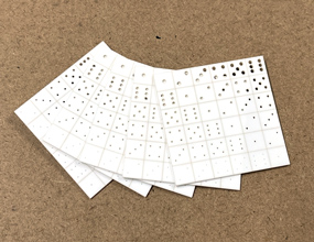
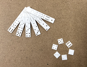
Combined Ceramic Scribing and Through-Hole Processing
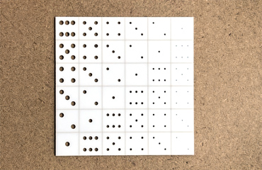
Laser scribing enables multiple small parts to be produced on a single panel. By keeping parts in panel through downstream processes, manufacturers can streamline production, reduce overall costs, and improve efficiency across the entire manufacturing workflow.
Scribing + Through-Holes
Material: Al2O3
Thickness: 0.635 mm
Hole Diameter: Ø 0.2 mm–Ø 1.0 mm
Scribe Depth: 0.24 mm
Individual Piece Size: 5 × 5 mm
Laser: CO2 Laser
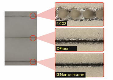
Scribe Line Comparison
Material: AlN
Thickness: 635 μm
Scribe Depth: 240 μm
Laser:
①CO2 Laser
(Line Width 105 μm)
②Fiber Laser
(Line Width 30 μm)
③Nanosecond Laser
(Line Width 28 μm)
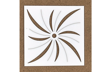
Curved Cutting in Alumina
Material: Al2O3
Substrate Size: 50 × 50 mm
Thickness: 1.0 mm
Laser: CO2 Laser
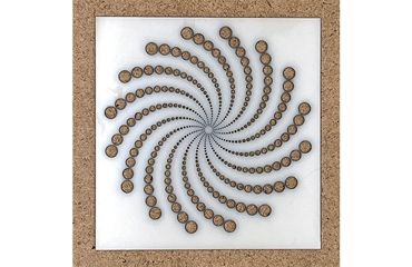
Small-Diameter, High-Hole-Count Machining in Ceramics
For components with high hole counts, we maintain consistent machining quality and productivity, backed by a manufacturing system designed for volume production.
Through-Holes Ø 0.1 mm and Larger
Material: AlN
Thickness: 0.38 mm
Hole Diameter: Ø 0.1 mm–Ø 2.7 mm
Laser: Fiber Laser
Extreme Precision
Smaller Holes. Higher Density.
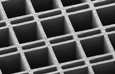
Micro-Hole and Ultra-Narrow Slit Machining
Hole Size: 14 × 70 μm
Material: Si3N4
Thickness: 200 μm
Aspect Ratio: 14.3
Corner Radius ≤3 μm
Laser: Femtosecond Laser
Narrow Pitch & Minimal Corner Radius
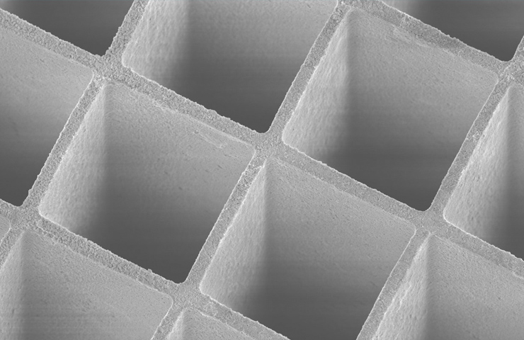
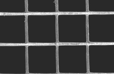
Wall Thickness ≤5 μm /
Corner Radius ≤3 μm
Material: Si3N4
Thickness: 381 μm
Hole Size: 55 × 55 μm
Laser: Femtosecond Laser
Complex Geometries
Create Virtually Any Shape
Control Hole Geometry with Precision
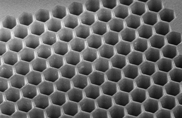
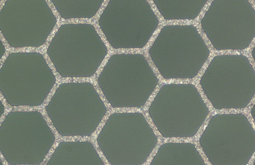
We can produce shapes that are difficult to achieve with die-based or conventional mechanical machining methods.
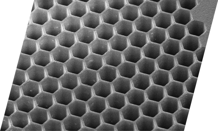
Hexagonal Hole (65 μm Across Flats)
Material: Si3N4
Thickness: 381 μm
Wall Thickness: ≤10 μm
Laser: Femtosecond Laser
High-Precision Profile Cutting
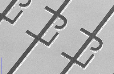
Application: Probe Pins and Similar Components
Material: Palladium Alloy Foil
Pin Size:
20 μm Width × 30 μm Thickness
Laser: Femtosecond Laser
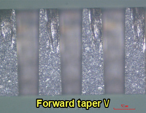
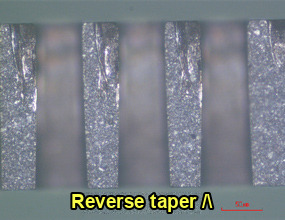
Precision Taper Control
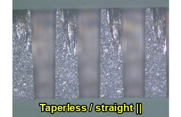
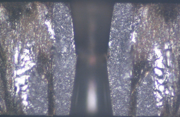
We can machine advanced hole geometries, including different entry and exit diameters and narrowed sections within the hole that are difficult to achieve using conventional processes.
Taper Control
Material: Si3N4
Thickness: 200 μm
Hole Size: 55 × 55 μm
Laser: Femtosecond Laser
Hourglass-Shaped Holes
Material: Si3N4
Thickness: 200 μm
Minimum Hole Diameter: Ø 50 μm
Maximum Hole Diameter: Ø 75 μm
Laser: Femtosecond Laser
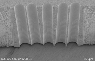
Hole Taper Angle: ≤ 5°
Material: Si3N4
Thickness: 381 μm
Hole Diameter: Ø 68 μm
Laser: Femtosecond Laser
Thick Materials. Fine Holes.
Micro-Hole Drilling in Thick Substrates
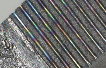
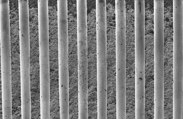
High-Aspect-Ratio Hole Machining (Round Holes)
Aspect Ratio: 20
Material: Si3N4
Thickness: 1,000 μm
Hole Diameter: Ø 50 μm
Laser: Nanosecond Laser
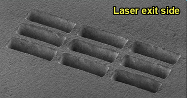
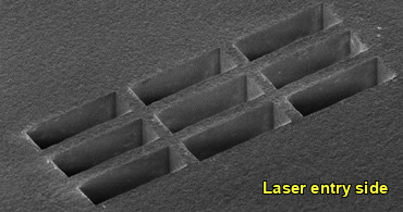
High-Aspect-Ratio Machining (Square Holes)
Aspect Ratio: 15.8
Material: Si3N4
Thickness: 635 μm
Hole Size: 40 × 140 μm
Laser: Femtosecond Laser
Blind Holes
Precise Depth Control
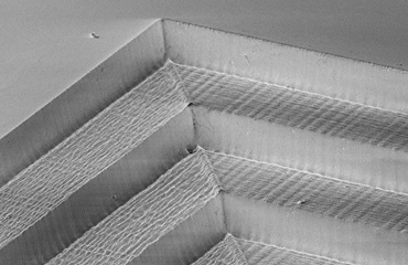
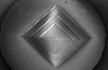
Stepped Recess Machining in Glass
Three-Step Counterbore
(80 μm Per Step)
Material: Glass
Hole Size: 1,000 × 1,000 / 800 × 800 / 600 × 600 μm
Laser: Femtosecond Laser
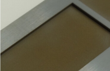
Counterbore Machining in Ceramics
Counterbore Depth: 450 μm
Material: Si3N4
Thickness: 600 μm
Flatness: ≤ 20 μm
Laser: Fiber Laser
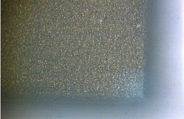
Counterbore Depth: 400 μm
Material: Al2O3
Laser: CO2 Laser
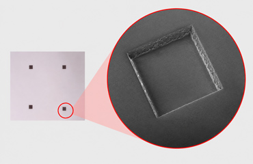
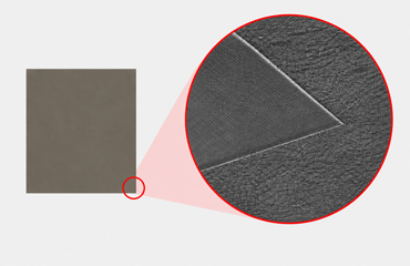
Counterbore Depth: 30 μm
Material: Al2O3
Laser: CO2 Laser
02 Question What materials can you machine?
We work with a wide range of materials..
Contact us to discuss feasibility.
ANSWER
- Machinable Materials
- Sheet Materials Up to
About 2 mm Thick
| Machinable Materials | Typical Materials |
|---|---|
| Single-Crystal Minerals | Diamond, Silicon, Sapphire, Zirconia and Others |
| Ceramics | Alumina, Aluminum Nitride, Silicon Nitride, Silicon Carbide and Others |
| Glass | Soda-Lime Glass, Borosilicate Glass, Quartz Glass and Others |
| Metals | Stainless Steel, Titanium, Tungsten, Molybdenum, Steel and Others |
| Polymers | Epoxy (Glass Epoxy), Polyimide, Engineering Plastics and Others |
Ask us about materials
not listed here
Even Diamond
Can Be Machined
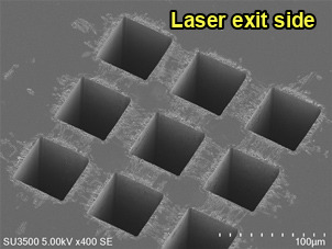
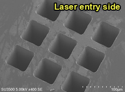
Square-Hole Machining in Diamond
Material: Diamond
Thickness: 300 μm
Hole Size: 40 × 40 μm
Laser: Femtosecond Laser
03 Question What Can Laser Micromachining Be Used For?
Electronics Continue to Become Smaller and More Powerful.
Micron-level precision is now the standard.
Ready to meet the demanding requirements of semiconductor, AI, and EV applications.
ANSWER
Semiconductors and Next-Generation Electronics APPLICATION 01

- Semiconductor Test Equipment (Probe Cards)
- We machine guide plates in silicon nitride and machinable ceramics to ultra-high accuracy, achieving ±2 μm on position and ±1 μm on hole diameter. Our work includes fine square holes cut with ultrashort-pulse lasers, and probe pins made from palladium alloy foil.
- Semiconductor Manufacturing Components (Electrostatic Chucks)
- We drill deep, straight holes for electrostatic chucks used in silicon wafer handling, achieving aspect ratios of up to 20.
- AI and Advanced Computing Devices
- We produce high-density micro-hole patterns in ceramic substrates such as aluminum nitride (AlN), a heat-dissipation material used in AI semiconductors.
- Advanced Semiconductor Packaging (Chiplets)
- Advanced semiconductor packaging depends on high-density interconnect substrates (interposers), where ultrashort-pulse laser technology enables the precise formation of fine through-holes (vias). Beyond silicon, high-speed, high-precision machining of next-generation glass, polymer, and ceramic substrates is attracting growing attention.
Mobility & Infrastructure APPLICATION 02

- Automotive and Marine Sensors
- We perform precision laser micromachining of ceramic components used in a wide range of automotive and marine sensors.
- Next-Generation Mobility (EVs & Electrification)
- We contribute to the production of high-performance automotive components, including slit machining of silicon nitride substrates for EV applications.
- Communications Infrastructure Equipment
- Our technology is also applied to precision machining of electronic components used in communications infrastructure equipment such as base stations.
Advanced Materials & Process Development APPLICATION 03
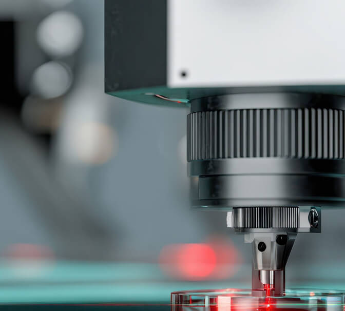
- Machining Advanced and Difficult-to-Process Materials
- We machine an exceptionally wide range of materials, including ceramics such as alumina, metals, single-crystal materials such as diamond and sapphire, a variety of glass materials, difficult-to-machine metals such as tungsten and molybdenum, and polymers including polyimide.
- Special Geometries and Taper Control
- We produce specialized features including square holes in diamond, multi-step counterbores in glass and silicon nitride, honeycomb structures (hexagonal holes) with wall thicknesses below 10 μm, and ultra-narrow slits just 14 μm wide. We also possess the expertise to precisely control laser-induced taper, creating straight-wall or reverse-taper geometries.
04 Question Can You Prototype? Can You Scale to Production?
We can prototype from a single piece.
Our extensive equipment lineup supports volume production with comprehensive quality assurance.
ANSWER
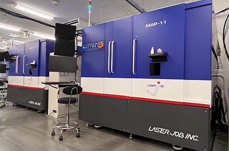
Laser Machines
Approx. 30 Units
We operate a wide range of laser systems, including CO₂, fiber, UV, green, nanosecond, and femtosecond lasers.
Our in-house developed laser processing equipment can also accommodate requirements that are difficult to achieve with standard commercial systems.
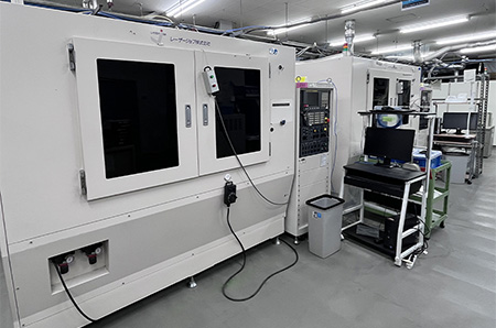
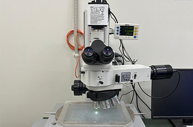
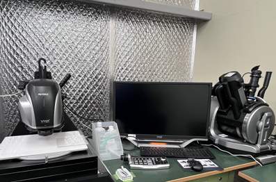
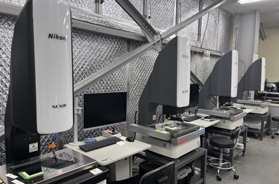
Measurement & Inspection Equipment
Approx. 30 Units
Certified to ISO 9001 and ISO 14001, we deliver products that meet our rigorous internal quality standards.
We support statistical process control (SPC) and full traceability to meet the stringent quality requirements of the semiconductor application.
Our controlled volume-production capability ensures consistent quality and reliable delivery.
- SPC
- Traceability
- Capable of 100% Inspection
Start with a Consultation
*To prepare a test prototype, we’ll request your design information
and may conduct a brief consultation to better understand your requirements.
05 Question Not Sure It’s Possible?
When the machining gets difficult, that’s where Laser Job excels.
If any of these situations sound familiar, we’d be happy to discuss them with you.
ANSWER

- •Another supplier turned the job down
- •You're not sure which machining process is right for your material
- •Your geometry or specifications are too specialized for standard production equipment
- •The required tolerances are so tight that you can't find a qualified supplier
- •You're struggling to establish machining conditions that deliver consistent quality
- •You've hit a technical challenge that requires deep expertise and experience to overcome
06 Question How Long Will It Take?
First, let us assess the feasibility of your application..
From initial consultation through final specifications, delivery in as little as two weeks may be possible.
ANSWER

Inquiry (No Drawings Required)

Review and Proposal

Quotation and Order

Machining and Delivery
Short Lead Time?
We May Be Able to Help.
Consultation Request Form
Please write in English or Japanese. We reply within 2–3 business days.

2-3-12 Bijogi-Kita, Toda-shi, Saitama 335-0038, Japan
TEL +81-48-422-4170 /
FAX +81-48-422-4175